What are the advantages and disadvantages of Integrated Circuits?
Integrated Circuits are defined as the circuit that comprises elements that are inseparable and interconnected electrically in such a way that the IC cannot be separated for the reason of commerce and construction. Myriad technologies can be used to build such a circuit. Today what we call an IC, was originally known as a monolithic integrated circuit. It is believed that Kilby created the first working IC back in 1958 and he won the Nobel Prize in Physics in 2000 for his hard work. The first buyer for this invention was the US Air Force. This article discusses an overview of the integrated circuit and its working.How are Integrated Circuits Made?
How do we build a memory or processor chip for a computer? It all starts with a raw compound element such as silicon, which is chemically treated or doped to create it and it has different electrical properties.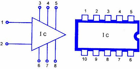
Integrated Circuit Symbol
Doping Semiconductors
Conventionally, people think about equipment fitting into two neat categories: those that allow electricity to flow through them quite readily (conductors) and those that don’t (insulators). Metals make up most of the conductors, while nonmetals such as plastics, wood, and glass are insulators.
In fact, the effects are far more complex than this, particularly when it comes to defining elements in the center of the periodic table (in groups 14 and 15), notably silicon and germanium. Usually, insulators are the elements that are prepared to perform more like conductors if we insert small quantities of impurities into them in a procedure known as doping.
Integrated Circuit Design
If you add antimony to silicon, you provide it slightly extra electrons than it would usually include the power to conduct electricity. Silicon “doped” that way is called n-type silicon. When you add boron instead of antimony, you take away some of silicon’s electrons, leaving behind “holes” that work as “negative electrons”; next, transport a positive electric current in the opposite way.
Such type of silicon is called p-type. Putting areas of n-type and p-type silicon side by side to create junctions wherein electrons act in very attractive ways is the way in which we generate electronically, semiconductor devices like diodes, transistors, and memories.
Inside a Chip Plant
The procedure of manufacturing an integrated circuit starts with a big single crystal of silicon, shaped like a long solid pipe, which is “salami sliced” into thin discs (about the size of a compact disc) called wafers.
The wafers are marked out in a lot of identical square or rectangular areas, each of which will build up a single silicon chip (sometimes called a microchip). Thousands, millions, or billions of apparatus are then produced on each chip by doping dissimilar areas of the surface to turn them into n-type or p-type silicon.
Doping is completed by a multiplicity of different processes. In one of them, known as sputtering, ions of the doping material are fired at the silicon wafer just like bullets from a gun. One more procedure called vapor deposition involves introducing the doping material as gas and letting it concentrate such that the impurity atoms generate a thin film on the surface of the silicon wafer. Molecular beam epitaxial is a much more accurate form of the statement.
Of course, building-integrated circuits that pack hundreds, millions, or billions of apparatus onto a fingernail-sized chip of silicon is all a bit more difficult than it sounds. Imagine the chaos when a dot of dirt could reason when you work at the microscopic (or sometimes even the Nanoscopic) scale. That’s why semiconductors are prepared in spotless laboratory environments called clean rooms, where the air is scrupulously filtered and employees have to pass in and out through airlocks exhausting all kinds of protecting clothing.
Construction
The steps involved while manufacturing an integrated circuit are two like fabrication and packaging.
· Fabrication
· Packaging
Fabrication
Fabrication is nothing but the procedure of making ICS or integrated circuits. It is a series of chemical as well as photographic steps where different circuits are designed over a semiconductor material called a wafer. The different steps involved in fabrication include the following.
Lithography
In lithography, a photo-resisting liquid layer is applied on the outside of the wafer/semiconductor. After that, it is backed as well as hardened.
Etching
In this procedure, unnecessary material can be detached from the wafer. After that, the photo-resist model is transferred toward the wafer.
Deposition
In a deposition, different materials films are applied over the wafer and this process can be done through two deposition methods either Chemical Vapor or Physical Vapor.
Oxidation
In this method, the Si layers on the summit are changed to Sio2 through oxygen otherwise water molecules.
Diffusion
Diffusion can be carried out toward annealing lattice faults.
Packaging
An alternate name of packaging is assembly or encapsulation.
It is the last phase while manufacturing IC. In the starting, the packaging of ICs can be done within ceramic flat packs. So this method was mainly used for several years after that the Dual-in-line package or DIP was introduced. After some days, other methods were introduced like Pin Grid Array & Surface mount. AMD & Intel have shifted to land Grid array packages. The packaging procedure includes some steps that have to follow some steps like the following.
· Attaching of Die
· Bonding of IC
· Flip Chip
· Quilt Packaging
· Attaching of Film
· Encapsulation of IC
Mostly, ICS are packaged in ceramic insulation/ opaque plastic. In the packaging, there are metal pins, used for connecting to the external world.
IC Design
There are different logic methods available for specific circuit design for designing an integrated circuit. In IC design, there are two categories which include the following.
· Digital design
· Analog Design
In the digital design method, memories like ROM, RAM, FPGA, Microprocessors are designed. This type of design ensures that the circuits are accurate & their density is at the highest. The circuit’s complete efficiency is extremely high.
Alternatively, Analog design is used to design filters, oscillators, op-amps, PLLs (phase-locked loops) & line regulators. This kind of design plays a key role wherever power dissipation, resistance & gain are required to be faultless. These circuits are designed by using automated design tools because the demand for design is alarmingly increasing & designs need to be made extremely quickly. In the design process, there are some steps that need to follow like the following.
· Estimation of Size & Possibility report
· Design of Circuit
· Simulation of Circuit
· Floor Planning
· Design Review
· Layout Design
· Analysis of Timing
· Generation of Automatic Test Model
· Manufacturing Design
· Preparation of Mask Data
· Wafer Fabrication
· Die Test
· Packaging
· Characterization of Device
· Data Sheet Generation
· Last Production
· Reliability Analysis
· Failure Analysis
The digital design includes ESL Design where the user creates specifications in it by using programming languages like C++, Matlab, Verilog, etc. After that, the user specifications within the ESL design are changed into RTL (Register Transfer Level) description. In RTL design, it defines the interconnections toward the inputs & outputs. The final design is Physical Design where the final chip design can be created through the logic gates & RTL.
The circuit simulation tools in analog design are mainly used to design the integrated circuits through high efficiency to make difficult calculations. If there are any errors while designing the cycle, then circuit simulation tools are used to locate & fixed them before the fabrication method. Some other factors like the concentration of doping & temperature can be continuously monitored to decide if the IC design is prepared to be made-up.
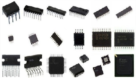
Types of Integrated Circuits
The different types of an integrated circuit which includes the following
Digital Integrated Circuits
This kind of IC has two defined levels:1’s and 0’s which implies that they work on binary mathematics wherein 1 stands for on and 0 stands for off. Such ICs are accomplished diligently as they contain more than millions of flip flops, logic gates, and whatnot, all incorporated into a single chip. Examples of digital IC include micro-controllers and microprocessors.
Types of Integrated Circuits
· Logic ICs
· Memory Chips,
· Interface ICs (level shifters, serializer/de-serializer, etc.)
· Power Management ICs
· Programmable Devices
Analog Integrated Circuits
The analog integrated circuits work by tackling continuous signals and are capable of performing tasks such as filtering, amplification, demodulation, and modulation, etc. Sensors, OP-AMP’s are essentially Analog ICs.
· Linear IC’s
· RF IC’s
Mixed Signal
When the digital and analog ICs are used on a single chip; the resultant IC is known as mixed-signal integrated circuits.
· Data Acquisition ICs (including A/D converters, D/A converter, digital potentiometers)
· Clock/timing IC’s
Uses of Integrated Circuits
The integrated circuit uses a semiconductor material (read chips) as the working table and frequently silicon is selected for the task. Afterward, electrical components such as diodes, transistors, and resistors, etc. are added to this chip in minimized form. Electrical components are joined together in such a way that they are able to carry out multiple tasks and calculations. The silicon is known as a wafer in this assembly.
Why is Integrated Circuits Important?
The IC or integrated circuit includes thousands to millions of electronic components such as resistors, transistors & capacitors which are fabricated onto a single chip. At present, almost every device like cell phones, TVs, computers, digital watches utilizes integrated circuits because of their tiny size as well as high efficiency & reliability. So, without using ICs, electronic gadgets will become slow and bulk. So this is the reason to use the integrated circuits in different applications.
Advantages
The advantages of the integrated circuits include the following.
· Small size
· Power consumption is less
· Reliability
· Less cost
· Less weight
· Replacement can be done very easily
· More consistent
· Improved operating speed & performance
· It operates at high temperatures
· Appropriate for small signal operation
Disadvantages
The disadvantages of the integrated circuits include the following.
· The integrated circuit handles simply a limited amount of power.
· The power dissipation is restricted to 10 watts
· In this, high rating PNP assembly is not achievable.
· High voltage operation & less noise are not simply obtained.
· A low-temperature coefficient cannot be achieved
· The indicators/ coils cannot be made-up.
· Delicate
Applications of Integrated Circuits
The applications of an IC’s includes the following
· Radar
· Wristwatches
· Televisions
· Juice Makers
· PC
· Video Processors
· Audio Amplifiers
· Memory Devices
· Logic Devices
· Radio Frequency Encoders and Decoders
In this article, we have discussed an overview of the integrated circuit briefly including types of integrated circuit and advantage and disadvantages of integrated circuit, and so on. Two types of methods have been used to build integrated circuits with the help of a doping semiconductor, inside a chip plant. We have dealt with the different types of integrated circuits like digital integrated circuits, analog integrated circuits, and finally mixed signals with examples. In addition uses of integrated circuits and applications of integrated circuits have also been discussed.
Furthermore, for any queries regarding this concept or to implement the electrical and electronics projects, please give your valuable suggestions by commenting in the comment section below.